From 2D materials to real-world applications: Next-2Digits moves forward
November 2, 2026Following the second project review, Next-2Digits is entering an important phase of its journey from advanced 2D materials towards integrated photonic devices and real-world applications. Over the recent project period, the consortium has continued advancing the technologies needed to integrate graphene and other 2D materials into photonic platforms at wafer scale. The work has progressed from material preparation and transfer towards wafer-scale integration, device fabrication and, increasingly, system-level validation.
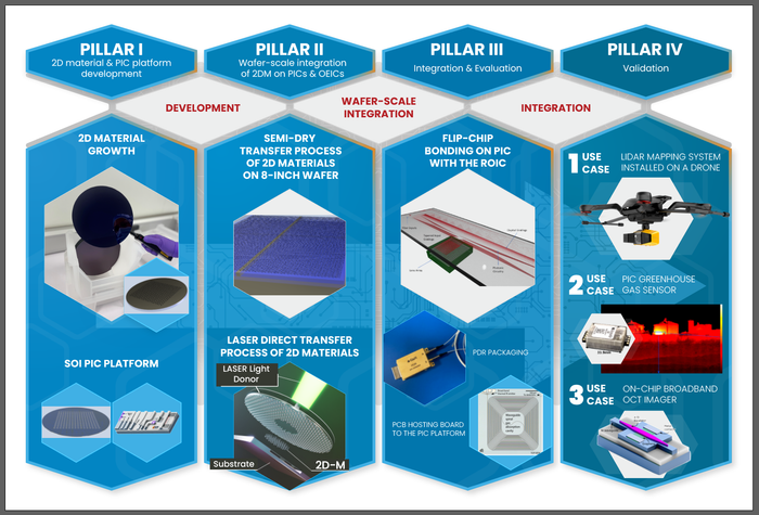
Progress across the technology chain
An important focus of Next-2Digits is developing scalable approaches that can bridge the gap between promising 2D materials and their practical integration into photonic technologies.
Recent progress includes:
- Wafer-scale graphene integration, with activities progressing on both 6- and 8-inch platforms.
- Complementary transfer technologies, including further development of semi-dry transfer and Laser Digital Transfer approaches.
- Integration into photonic devices and circuits, bringing the transferred materials closer to functional components and systems.
- Application-oriented development, connecting the integration technologies with the requirements of the project’s three use cases.
Together, these developments support the transition from individual technology and component demonstrations towards more integrated systems.
Moving towards three targeted applications
Next-2Digits is demonstrating its technologies through three application areas: LiDAR, gas sensing and Optical Coherence Tomography (OCT). Each use case provides a different environment in which the potential of 2D-material-enabled photonics can be explored, from sensing to imaging. As the project progresses, increasing attention is therefore being placed on integration, performance and validation at system level.
The next phase
There is still important work ahead. The individual technologies and components now need to come together and demonstrate the performance required by the targeted applications. However, the progress achieved so far provides a strong foundation for this next phase. By connecting advances in wafer-scale integration and transfer technologies with photonic devices and application-driven validation, Next-2Digits continues working towards its overall goal of bringing 2D materials closer to practical photonic applications.
Step by step, Next-2Digits is moving 2D-material-enabled photonics from advanced research towards real-world sensing and imaging applications.